English

 Spanish
 Japanese
 Korean
 German

+1 (408) 571 8651
(086)+1 (408) 571 8651

In the fields of optical manufacturing and semiconductor fabrication, precision cutting plays a decisive role in determining product quality and production efficiency. As components become smaller, thinner, and more complex, traditional cutting tools often struggle to meet the required tolerance and surface finish. This is where the wire saw emerges as a leading solution, offering unmatched precision, minimal material loss, and versatility for a wide range of hard and brittle materials such as sapphire, silicon carbide, quartz, and optical glass.

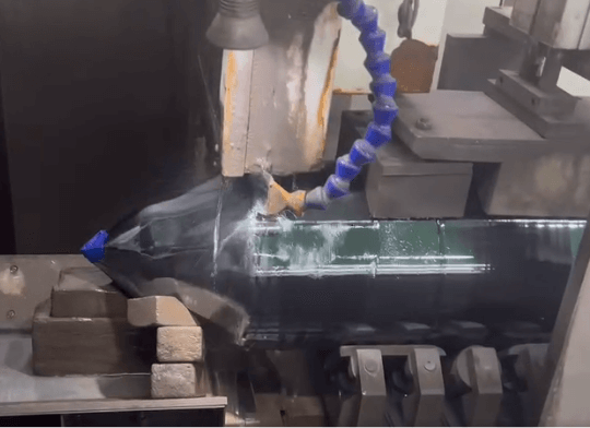
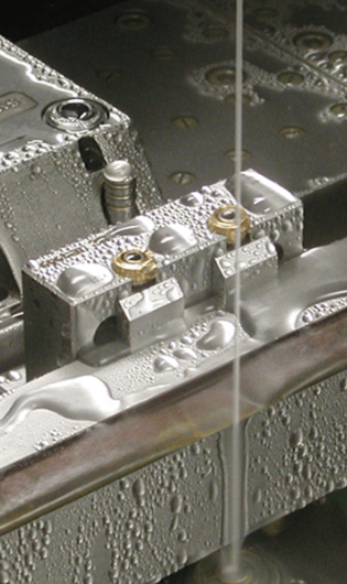
A wire saw uses a thin, diamond-coated wire loop or spool to cut through materials with exceptional accuracy. The diamond abrasive particles are firmly embedded on the wire surface, allowing the tool to slice through ultra-hard materials without generating excessive stress or heat. In advanced optical and semiconductor applications, the wire saw’s cutting process is optimized through CNC control, automatic tensioning, and variable wire speed to match the material’s characteristics.
Cutting Medium: Either dry cutting with dust extraction or wet cutting with a controlled coolant system.
Wire Speed: Up to 80 m/s for high-speed material removal while maintaining precision.
Cutting Tolerance: Achievable within ±0.03 mm, with positioning accuracy as fine as ±0.01 mm.
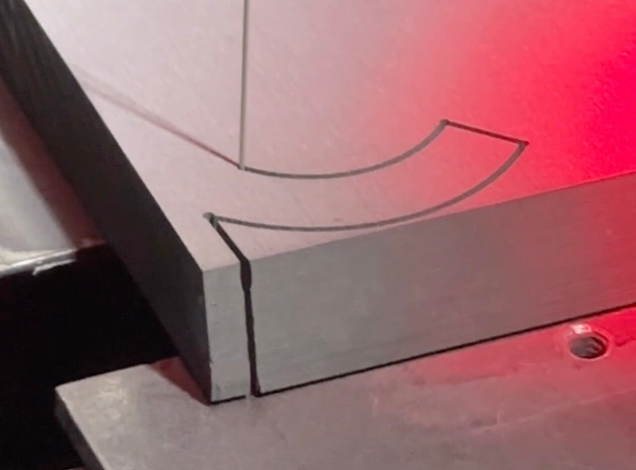
Optical components—such as lenses, filters, prisms, and infrared windows—require a cutting method that minimizes chipping, surface defects, and internal stress.
Key benefits of using a wire saw in optics include:
Ultra-Smooth Surfaces – Reduces the need for extensive post-polishing.
Minimal Kerf Width – As low as 0.4 mm, preserving expensive optical materials.
Capability for Complex Shapes – CNC programming enables precise contour cuts for specialized optical designs.
Consistent Repeatability – Ensures batch-to-batch uniformity in production.
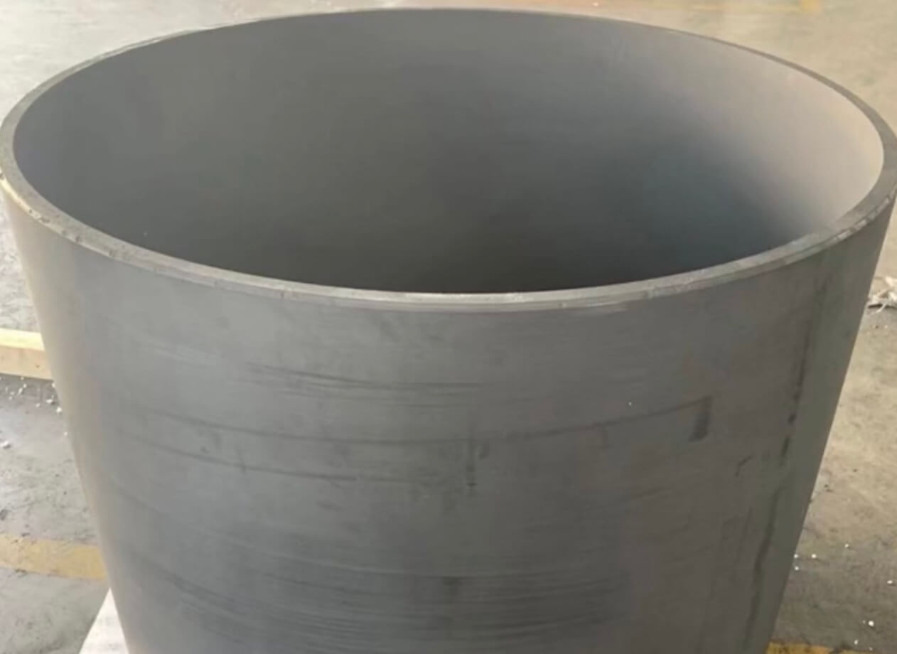
In semiconductor manufacturing, material yield and wafer quality directly affect device performance. The wire saw is widely used for slicing silicon ingots, sapphire substrates, and other crystalline materials used in LEDs, microchips, and advanced sensors.
Low Subsurface Damage – Preserves crystal integrity and reduces microcracks.
High Material Utilization – Narrow kerf width maximizes the number of wafers per ingot.
Flexible Diameter Capability – Can handle small wafers for R&D or large ingots for mass production.
Cleanroom Compatibility – Optional dust-proof and water-proof machine designs for contamination control.
When compared to inner diameter (ID) saws or blade saws, the wire saw offers several measurable advantages:
Higher Precision – Wire saws maintain accuracy over long cutting cycles without blade warping.
Lower Material Loss – Reduced kerf width results in significant cost savings for high-value materials.
Broader Material Range – Capable of cutting ceramics, quartz, and advanced composites that challenge traditional saws.
Longer Tool Life – Endless diamond wire loops experience less wear than abrasive blades.
Selecting the appropriate wire saw depends on the material type, required thickness, and production volume.
Laboratory Research: Compact desktop models such as CNC-controlled systems are ideal for R&D and prototyping.
Small-Scale Production: Mid-size gantry-type machines provide versatility for both slicing and shaping.
Mass Production: Large-format wire saws handle bigger ingots and high-throughput operations while maintaining precision.
Additional considerations include automation level, wire diameter, cooling method, and worktable size customization.
The wire saw has become an indispensable tool in high-precision cutting for optical and semiconductor industries. Its ability to produce clean, accurate cuts with minimal material waste makes it ideal for manufacturing delicate optical components and high-quality semiconductor wafers. As industry demands push for higher precision and efficiency, wire saw technology continues to evolve—offering greater automation, faster cutting speeds, and improved surface finishes.